Example: SPI Master Communication
The core logic of this tutorial applies to all ESP32 boards, but all the operation steps are explained using the example of the Waveshare ESP32-S3-Zero mini development board. If you are using a development board of another model, please modify the corresponding settings according to the actual situation.
This tutorial introduces how to use the ESP-IDF SPI master driver, demonstrating the bus + device two-layer model, automatic chip select (CS) management, and how to choose pins for maximum clock speed. The example short-circuits the MOSI and MISO of the SPI2 bus with a jumper wire, forming a self-loopback circuit.
1. SPI Peripheral

SPI (Serial Peripheral Interface) is a high-speed, full-duplex synchronous serial communication protocol, commonly used for connecting Flash, displays, SD cards, sensors, and other peripherals that require higher bandwidth. Key features:
- Four-wire interface: SCK (clock), MOSI (Master Out Slave In), MISO (Master In Slave Out), CS (Chip Select).
- Master-slave architecture: The master generates the clock, controls CS, and initiates all transfers. Slaves are distinguished by their CS lines.
- Full-duplex: 1 bit of data can be simultaneously sent and received in each clock cycle.
- High speed: Typically reaches tens of MHz, far exceeding I2C and UART.
ESP32-S3 has 4 built-in SPI controllers:
| Controller | Purpose |
|---|---|
| SPI0, SPI1 | Internal use for accessing external Flash and PSRAM. Not available to applications. |
| SPI2 (a.k.a. FSPI) | General-purpose SPI controller, can act as master or slave. Used in this example. |
| SPI3 | General-purpose SPI controller, can act as master or slave. |
1.1 IO MUX vs. GPIO Matrix Impact on SPI Speed
On ESP32-S3, each SPI controller has a set of dedicated IO MUX default pins, and signals can also be routed to any other GPIO via the GPIO matrix (see GPIO Matrix and IO_MUX Pins). The two approaches yield different maximum clock speeds:
| Pin Routing Method | Max Reliable Clock for SPI Master on ESP32-S3 |
|---|---|
| IO MUX default pins | 80 MHz |
| GPIO matrix | 40 MHz |
SPI2 (FSPI) IO MUX default pins on ESP32-S3:
| Signal | GPIO |
|---|---|
| CS0 | 10 |
| SCLK | 12 |
| MISO | 13 |
| MOSI | 11 |
As long as the pins specified in the driver match the table above exactly, the driver will automatically use the IO MUX — no additional configuration required. Otherwise, it will automatically fall back to the GPIO matrix, limiting the speed to 40 MHz.
This example uses the default pins listed above so that it can directly benefit from IO MUX when high speed is needed.
1.2 General Steps: Bus + Device Model
The ESP-IDF SPI master driver uses a bus + device two-layer abstraction:
- Bus corresponds to the SPI controller and the shared SCK / MOSI / MISO signal lines, identified by
spi_host_device_t(e.g.,SPI2_HOST). - Device corresponds to a specific slave on the bus, described by
spi_device_handle_t. Each device has its own CS pin, clock frequency, SPI mode, and queue depth configuration — the driver automatically switches to the current device's configuration before each transfer.
This means multiple devices with different clock speeds and CS pins can share the same bus, and the driver manages everything automatically.
General steps:
-
Include header file
#include "driver/spi_master.h"And declare the dependency in
main/CMakeLists.txt:REQUIRES esp_driver_spi. -
Initialize the bus: Fill in
spi_bus_config_t(MOSI / MISO / SCLK pins, max transfer bytes, DMA channel) and callspi_bus_initialize(). Pass-1for unused pins (e.g., MISO in a write-only scenario). -
Add a device: Fill in
spi_device_interface_config_t(CS pin, SPI mode 0~3, clock speed, queue depth, etc.) and callspi_bus_add_device()to get a device handle. -
Initiate a transfer: Construct an
spi_transaction_t(data length, TX/RX buffers) and send it via one of these two APIs:spi_device_polling_transmit(): Polling — the calling thread busy-waits until completion. Best for short, low-latency transfers.spi_device_transmit(): Interrupt-driven — the calling thread blocks and yields the CPU. Best for long or infrequent transfers.
-
(Optional) Release resources:
spi_bus_remove_device()thenspi_bus_free().
CS is automatically managed by the driver. As long as spics_io_num is set in the device configuration, the driver will automatically pull CS low before each *_transmit() call and pull it high after completion — no manual GPIO operations needed in user code.
2. Example Project
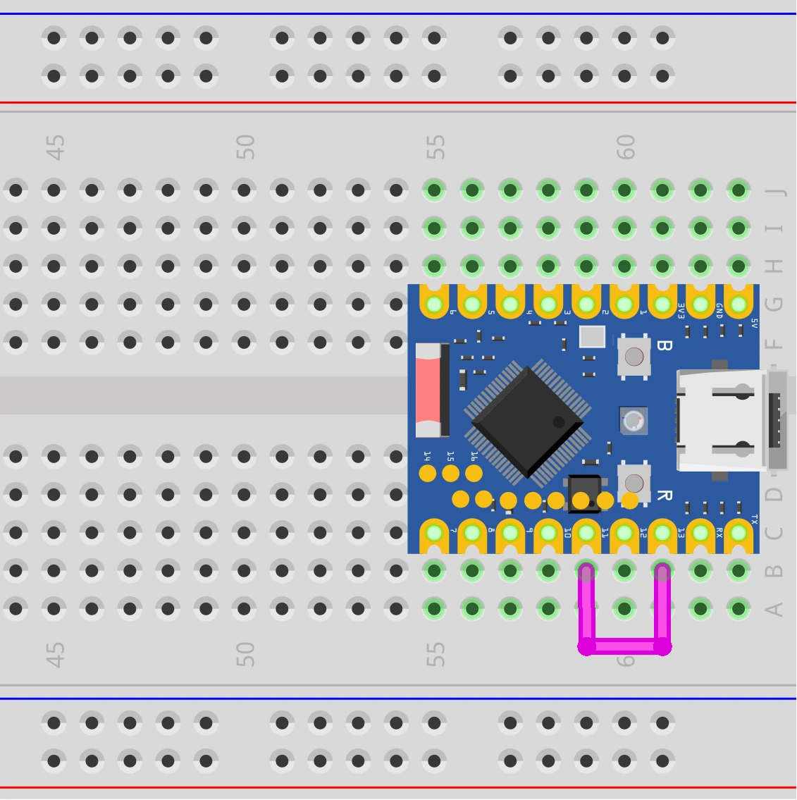
This example configures SPI2 as a master and short-circuits MOSI (GPIO11) and MISO (GPIO13) with a jumper wire to form a loopback circuit. The program sends a fixed data pattern in each transaction and receives it back, then compares whether the sent and received data match.
Since SPI is full-duplex, TX and RX happen simultaneously in one transaction — every bit sent on MOSI is immediately received back on MISO via the jumper in the same clock cycle. Comparing both sides verifies whether the entire SPI link is working correctly.
2.1 Circuit
Components required:
- Jumper wire
- ESP32 development board (Waveshare ESP32-S3-Zero Mini Development Board)
Use a jumper wire to short GPIO11 (MOSI) and GPIO13 (MISO). SCLK (GPIO12) and CS (GPIO10) do not need external wiring — the driver will automatically output the corresponding signals.
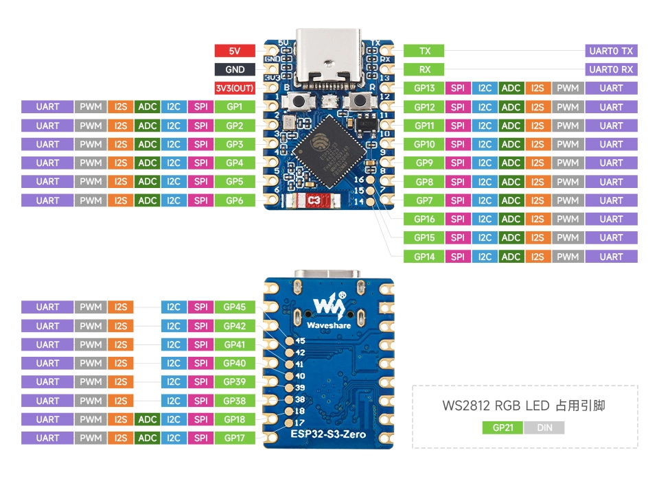
ESP32-S3-Zero Pinout Diagram
2.2 Create Project
-
Create a project. If you are not sure how to do this, refer to Create a Project from Template.
-
Refer to the SPI Master Driver API Reference. Follow the guidance in the documentation to complete the following steps.
First, include the header file in main.c:
#include "driver/spi_master.h"Then declare the
esp_driver_spicomponent in main/CMakeLists.txt:idf_component_register(SRCS "main.c"INCLUDE_DIRS "."REQUIRES esp_driver_spi)
2.3 Example Code
#include <string.h>
#include "freertos/FreeRTOS.h"
#include "freertos/task.h"
#include "esp_log.h"
#include "esp_err.h"
#include "driver/gpio.h"
#include "driver/spi_master.h"

static const char *TAG = "example";

#define SPI_HOST_USED   SPI2_HOST           // Use SPI2 (FSPI)
#define PIN_MOSI        GPIO_NUM_11         // FSPI IO MUX default pins
#define PIN_MISO        GPIO_NUM_13
#define PIN_SCLK        GPIO_NUM_12
#define PIN_CS          GPIO_NUM_10
#define SPI_CLOCK_HZ    (1 * 1000 * 1000)   // 1 MHz, easy to observe on oscilloscope
#define SPI_BUF_SIZE    16                  // TX/RX buffer size in bytes

static spi_device_handle_t dev_handle;

static void spi_init(void)
{
    // 1. Initialize the bus
    spi_bus_config_t bus_cfg = {
        .mosi_io_num     = PIN_MOSI,
        .miso_io_num     = PIN_MISO,
        .sclk_io_num     = PIN_SCLK,
        .quadwp_io_num   = -1,              // Not used in this example, set to -1
        .quadhd_io_num   = -1,
        .max_transfer_sz = SPI_BUF_SIZE,    // Max transfer bytes per transaction, aligned with actual buffer
    };
    ESP_ERROR_CHECK(spi_bus_initialize(SPI_HOST_USED, &bus_cfg, SPI_DMA_CH_AUTO));

    // 2. Add device
    spi_device_interface_config_t dev_cfg = {
        .clock_speed_hz = SPI_CLOCK_HZ,
        .mode           = 0,                // SPI mode 0 (CPOL=0, CPHA=0)
        .spics_io_num   = PIN_CS,           // CS automatically managed by driver
        .queue_size     = 1,
    };
    ESP_ERROR_CHECK(spi_bus_add_device(SPI_HOST_USED, &dev_cfg, &dev_handle));
}

void app_main(void)
{
    spi_init();

    // Prepare TX and RX buffers
    uint8_t tx_buf[SPI_BUF_SIZE] = {
        0x00, 0x11, 0x22, 0x33, 0x44, 0x55, 0x66, 0x77,
        0x88, 0x99, 0xAA, 0xBB, 0xCC, 0xDD, 0xEE, 0xFF,
    };
    uint8_t rx_buf[SPI_BUF_SIZE];

    while (1) {
        memset(rx_buf, 0, sizeof(rx_buf));

        spi_transaction_t trans = {
            .length    = sizeof(tx_buf) * 8,    // Unit is bits
            .tx_buffer = tx_buf,
            .rx_buffer = rx_buf,
        };

        ESP_ERROR_CHECK(spi_device_polling_transmit(dev_handle, &trans));

        // In loopback, rx_buf should be identical to tx_buf
        if (memcmp(tx_buf, rx_buf, sizeof(tx_buf)) == 0) {
            ESP_LOGI(TAG, "Loopback OK: %d bytes echoed back correctly",
                     (int)sizeof(tx_buf));
        } else {
            ESP_LOGW(TAG, "Loopback mismatch! Check jumper between GPIO%d and GPIO%d.",
                     PIN_MOSI, PIN_MISO);
            ESP_LOG_BUFFER_HEX(TAG, tx_buf, sizeof(tx_buf));
            ESP_LOG_BUFFER_HEX(TAG, rx_buf, sizeof(rx_buf));
        }

        vTaskDelay(pdMS_TO_TICKS(1000));
    }
}
2.4 Build and Flash
-
Configure flash options
Before building and flashing, make sure to check and set the correct target device, serial port, and flash method. Refer to Section 2 Run Demo - 1.3 Configure Project.

-
Click
 to automatically build, flash, and monitor in sequence.
 -
After flashing, make sure GPIO11 and GPIO13 are short-circuited with a jumper wire. The serial monitor should show periodic "Loopback OK" messages:
I (266) main_task: Calling app_main()I (276) example: Loopback OK: 16 bytes echoed back correctlyI (1276) example: Loopback OK: 16 bytes echoed back correctlyI (2276) example: Loopback OK: 16 bytes echoed back correctly...After disconnecting the jumper, you will see
Loopback mismatch!warnings with the sent and received data printed in hexadecimal.
2.5 Code Walkthrough
1. Include Header Files
#include "driver/gpio.h"
#include "driver/spi_master.h"
driver/spi_master.h: Entry point for the SPI master driver. Contains all needed types and APIs includingspi_bus_config_t,spi_device_interface_config_t, andspi_transaction_t. Belongs to theesp_driver_spicomponent.driver/gpio.h: Provides theGPIO_NUM_xenumerations.
2. Define Constants
#define SPI_HOST_USED   SPI2_HOST
#define PIN_MOSI        GPIO_NUM_11
#define PIN_MISO        GPIO_NUM_13
#define PIN_SCLK        GPIO_NUM_12
#define PIN_CS          GPIO_NUM_10
#define SPI_CLOCK_HZ    (1 * 1000 * 1000)
SPI2_HOST: Use the SPI2 controller. You could also useSPI3_HOST, but SPI3 on ESP32-S3 has no dedicated IO MUX pins — all pins go through the GPIO matrix, limiting the clock to 40 MHz.SPI1_HOSTis not available to applications (occupied by Flash).PIN_MOSI/PIN_MISO/PIN_SCLK/PIN_CS: Using SPI2's IO MUX default pins on ESP32-S3 (see Section 1.1). If you use different GPIOs, the driver automatically falls back to the GPIO matrix, reducing the max clock to 40 MHz.- The loopback doesn't require an external slave, but CS is still output normally by the driver (GPIO10 is pulled low with each transfer and pulled high when done). Keeping
PIN_CSensures the code structure is consistent with real slave scenarios — you only need to change the SPI mode and speed later without going back to add CS pin configuration. SPI_CLOCK_HZ: 1 MHz. This example is for loopback verification where speed isn't the bottleneck. A lower frequency makes it easy to observe waveforms on an oscilloscope or logic analyzer.
3. SPI Initialization (spi_init)
Completed in the order of "bus → device".
-
Bus Configuration (
spi_bus_initialize)spi_bus_config_t bus_cfg = {.mosi_io_num = PIN_MOSI,.miso_io_num = PIN_MISO,.sclk_io_num = PIN_SCLK,.quadwp_io_num = -1,.quadhd_io_num = -1,.max_transfer_sz = SPI_BUF_SIZE,};spi_bus_initialize(SPI_HOST_USED, &bus_cfg, SPI_DMA_CH_AUTO);mosi_io_num/miso_io_num/sclk_io_num: The three shared signal lines of the bus. Pass-1for unused pins (e.g., MISO in a write-only scenario).quadwp_io_num/quadhd_io_num: Not used in this example, always pass-1.max_transfer_sz: Maximum bytes per transfer. 0 uses the default value (4092). Setting it smaller saves DMA descriptor memory — this example aligns it with the actualSPI_BUF_SIZEbuffer.SPI_DMA_CH_AUTO: Let the driver automatically allocate a DMA channel. When transferring large blocks of data, DMA handles the transfer in the background so the CPU doesn't have to wait.
-
Device Configuration (
spi_bus_add_device)spi_device_interface_config_t dev_cfg = {.clock_speed_hz = SPI_CLOCK_HZ,.mode = 0,.spics_io_num = PIN_CS,.queue_size = 1,};spi_bus_add_device(SPI_HOST_USED, &dev_cfg, &dev_handle);clock_speed_hz: SCLK frequency for this device. The driver automatically selects the closest divider based on the clock source.mode: SPI mode 0~3, corresponding to CPOL/CPHA combinations. Mode 0 is CPOL=0, CPHA=0: SCLK is low when idle, data is sampled on the first clock edge (rising edge). This is the default mode for the vast majority of SPI slaves. Change this value if the slave's datasheet requires a different mode (e.g., mode 3).spics_io_num: CS pin number. When set, the driver automatically pulls it low before each transfer and high afterward. Set to-1to manage CS manually.queue_size: Number of transfer transactions that can be queued simultaneously. Set to 1 for polling mode; increase for pipelined transfers in interrupt mode.
The resulting dev_handle is used for all subsequent transfer calls.
4. Main Loop: Perform a Loopback Transfer
spi_transaction_t.length and .rxlength are both in bits, not bytes. When calculating length based on sizeof(), you need to multiply by * 8.
spi_transaction_t trans = {
    .length    = sizeof(tx_buf) * 8,
    .tx_buffer = tx_buf,
    .rx_buffer = rx_buf,
};
spi_device_polling_transmit(dev_handle, &trans);
.length: Transfer length, in bits, not bytes. 16 bytes = 128 bits..tx_buffer: Buffer containing the data to send..rx_buffer: Buffer to receive data into. Setting both TX and RX makes this a full-duplex transfer: N bits sent and N bits received simultaneously. To send without receiving, omit.rx_buffer(pass NULL).spi_device_polling_transmit(): Initiates a polling transfer — the calling thread busy-waits until completion. This is the simplest approach for this example's once-per-second small data transfers.
Since MOSI and MISO are short-circuited, every bit the master sends on MOSI immediately appears on MISO at the same clock edge and is sampled back. Ideally, rx_buf should be identical to tx_buf. Verification is done with memcmp().
If length > rxlength, the driver automatically assumes rxlength = length, i.e., receive and send are equal in length. If you want to send N bits but only receive M bits (M < N), explicitly set .rxlength = M * 8.